Foxconn C51XEM2AA 8EKRS2H
Jul 24th, 2006 | By Archive
Foxconn C51XEM2AA 8EKRS2H
Date
: 07/24/06 – 02:31:26 PM
Author
:
Category
: Motherboard
Page 1 : Index
Manufacturer: Foxconn
Price:
$209.99 USD (Newegg.com)
Here comes Foxconn and if you didn't listen last time, then you better pay attention this time around because the AM2 motherboard battle just got another heavy-weight contender. It seems like yesterday but nearly a year ago, last August, I looked at a Foxconn retail nForce4 SLI motherboard for socket 939 that piqued my interest. At the end of that review I said this:

It was like Foxconn was reading my mind because they went back to the drawing board and revamped their AMD line for the release of AM2 with a top-of-the-line nForce 590 SLI motherboard that looks poised to shake things up on the AM2 platform. The WinFast name appears to be gone and the humdrum look of their package has turned into an outright marketing assault with the introduction of the Foxconn C51XEM2AA-8EKRS2H.

Out with the old and in with the new might be the theme at Foxconn because this motherboard looks incredible. The package is clean, concise, and cunningly elegant. The AM2 platform is the newest out right now breaking AMD into the DDR2 world of memory. With the memory update, the chipsets also got a facelift and Foxconn decided to power the C51 with NVIDIA's nForce 590 SLI. There is plenty of new stuff to cover so no stalling.
Page 2 : Package & Contents
I hinted at the facelift the highest Foxconn offering received but you have no idea how much of a difference there is.

There was nothing wrong with the package that the NF4SK8AA came in but it certainly didn't exude top-of-the-line product machismo. This package does just that and so much more. First off WinFast is gone and Foxconn is proudly displayed in the prominent position. It is also obvious NVIDIA has dived head first into teaming up with Foxconn for this product, making this motherboard the 590 SLI reference design.

The contrasting white and black color mixed with the NVIDIA green provides a dynamic feeling for the whole package. At the same time, it maintains its sophistication without resorting to standard marketing themes. This larger substantial design provides the Foxconn C51 with immediate respect to anyone who picks this package up.

The ECS flagship Extreme edition comes with a sleeve, Asus flagship A8R32/A8N32/M2N32 motherboards all come with a sleeve, so why shouldn't Foxconn's number one motherboard? The excess of this type of package isn't really necessary but it seems to carry some sort of status symbol to the product to have a sleeved package. Every side of this box has the Foxconn name on it as well as "POWERED BY NVIDIA".

This is our mini specifications list that all motherboards are accompanied by. Retailers love it because they can pretend to know the specs of a motherboard while showing a customer, the whole time reading this little sticker… so sneaky.

With nothing more to look at on the front side, I turn the package around to the usual wall of diagrams, charts, and logos that reside on the backside of a motherboard package. With the close affiliation to NVIDIA on this product, it is no surprise to see that SLI gets heavy coverage back here.

SLI is not new and certainly not unique to this motherboard but it is still a major selling feature NVIDIA needs to utilize. Therefore, it will continue to get major air time on packages like this. The one thing to point out is that the 590 SLI chipset runs in SLI with both physical connections at a full x16 bandwidth.

This chart gives us a good breakdown of what the NVIDIA nForce chipset offers the Foxconn C51. I will go into detail about the nForce chipsets offered with AM2 motherboards in the specifications section.

This list sums up the attributes of socket AM2 for those who are unaware of the changes that have been implemented. The biggest, of course, is the switch to DDR2 memory from DDR. The rest of the AM2 platform is very similar to 939 with a few minor updates that will be outlined in the specifications section.

Hidden beneath the white optimistic sleeve of the C51 package lays a dark black interior. I hope the performance mimics the package and is dark and tough on the inside when it comes to overclocking. At this point the package has been covered and we jump inside.

Foxconn didn't change everything it appears as I am greeted with what I assume to be the familiar installation and setup poster that provides all the basic information one needs about the motherboard. Underneath the poster is a bubbling pile of packages that appears to be far more substantial than the NF4SK8AA.


All one can say is wow, or ouch I guess, if you consider that the price of the motherboard is likely marginally inflated due to this extensive package. Along the bottom, note that there are 6 SATA cables and all are black in color – very nice. Just above those are a pair of ribbon cables and at the top, expansion brackets that include a 4x USB, 6-pin/4-pin FireWire, and serial port bracket. The upper left shows 3 molex-to-SATA power adapters for up to 6 hard drives. I am not sure why there are so many of these but Foxconn must have found that people wanted these connectors. The last little bag is the SLI bridge in its ESD bag.


The only other contents inside the box aside from the motherboard itself are the manual, drivers and installation CD, as well as the rear I/O panel. The manual feels very thick and just leafing through, it appears to be quite detailed. It is definitely more than the token manual that some motherboards show up with.

Last, but certainly not least, is the motherboard itself which is packed securely in a sealed bag. Before I start fondling this nice looking board we will have a look at the specifications a little better than we did when going over the package.
Page 3 : Specifications
Until we re-design the web site and incorporate HTML into our articles, I will have to rely on images from manufacturers' web sites to list specifications. They are small GIF files so they shouldn't add to the load time of the page too much. Without any delay, our first look at the complete specifications list of the C51:

I won't go into much discussion regarding the specifications of the 590 SLI chipset but will mention the main differences from the nForce4 SLI/X16 chipset. Obviously, memory is DDR2 and not DDR. This means different memory speeds and the 590 handles 533 / 667 / 800. Other notable additions are the extra 2 SATAII connections along with the inclusion of RAID5. I might have to squeeze enough drives together and benchmark the RAID5 performance. That will depend on drive availability at my place. The only other noticeable enhancements are proprietary enhancements like NVIDIA LinkBoost technology, and NVIDIA EPP memory technology. Updates to the audio hardware are also part of the 590 SLI package.

The new Foxconn web site is nice for navigation and provides all the information we need but not much more. I do appreciate the large photo of the motherboard. Most all additional information about the features of this motherboard will be found in the Chipset section on the next page.
Page 4 : Chipset
With a new socket comes new chipsets and with new chipsets come new toys that will be built into the motherboard as well as updates to what has existed for years. The Foxconn C51 runs on the NVIDIA 590 SLI chipset which is king of the nForce 500 hill. The peasants include the 570 SLI, 570 Ultra, and 550 to round out the family.

Hey wait a minute, that lineup looks very similar to another set of options for socket 939. Some scoff, I say why not? It fills a bunch of potential markets and gives us a bunch of pricing options. Every feature has been improved upon from the nForce4 chipset on socket 939 and plenty of brand new features have been added. This section will concentrate on the advantages that the higher end chipsets have over the others seeing as the Foxconn C51 is the highest of them all.

If you look at the nForce 500 MCP feature list, you will see that there are only two advantages to the 590 SLI chipset. This is true and it isn't. There are a couple other underlying benefits that make it so much more. The first couple of enhancements are called
LinkBoost
and Certified SLI or
EPP Memory
.
LinkBoost
– simply put, LinkBoost overclocks the PCI-E bus 25% as well as the HT link 25% between the MCP and SPP. Higher-end NVIDIA video cards, of course, are required, such as a pair of 7900GTXs. This, in theory, opens up the bandwidth another 2GB/s providing further room for overclocking on the buses involved. This is all done automatically but I would imagine a BIOS setting would have to be enabled like the EPP does.
EPP Memory
– is another 'automatic overclock' technology that allows memory manufacturers to program various SPD sets that allow for "automatic overclocking". The ability to have three separate SPD profiles allows for more aggressive timing, higher voltage, and lower drive-strength settings to be used for the EPP enhanced setting while still having more relaxed settings so compatibility remains high amongst various motherboards. When enabled on a 590 SLI motherboard like the Foxconn C51, EPP memory will automatically be set to the pre-programmed timings and voltages for enhanced performance.
nForce 590 SLI Chipset

Starting at the top, DDR2 memory interfaces directly with the on-die memory controller on the CPU. Each 16X PCI-E link connects to one chipset, either the MCP or SPP. These two then interact by way of another HyperTransport link that runs off of a reference clock of 200 which is multiplied by up to 5 for a maximum of 1GHz but can be overclocked significantly as claimed by NVIDIA. The SPP then links to the CPU with the standard HyperTransport link that we had in 939 which ran and still runs at 1GHz.

- More control
- Ensures maximum overclockability
- Automatically set performance for key applications
- Play games or make VoIP calls without fear of disruption when you browse the net and download files.
- Faster file transfers
- Higher system performance (lower CPU utilization)

I think we have seen enough specifications, talked enough about potential, and discussed what is possible to extent. I want to see this board and get it running to see what it will actually do. Next up is the long and exhaustive photo journey that I call the Layout section.
Page 5 : Layout
My favorite part of any motherboard review is the layout section where there are photos-a-plenty and from the layout you can get a good feeling about a motherboard and what it can do.

We start with a high angle photo from what would be the front side of the motherboard when mounted in a case. The spacing looks decent although there are some tight spots and a couple things I don't like right off the bat. There are also some things that I am happy to see. The standout on this board is the bright green NVIDIA badged MCP chipset cooler. This is just another of the many signs that show NVIDIA endorses this motherboard.

With a new socket we get a new mount and in my opinion, it was a bit of an upgrade. The retention bracket now mounts at four points through the motherboard instead of the two that came with Socket 939. The socket itself has not changed but a few things around it have. Speaking of room around the socket, there isn't a whole lot between the socket and the first memory module but it is hard to say whether it will play a role with water or air cooling.

As always, directly to one side of the socket is our power station. The new AM2 boards seem to have brought a new standard as this is the second motherboard I have seen that comes with a 4-phase setup as opposed to the standard 3-phase system found on most Socket 939 boards.

Rubycon where it counts, seems to be the theme for Foxconn on this board as we can see by the photo above. Right in the middle of capacitors are the Falco power inductors. The inductors are shielded and have a current rating up to 30.30A. These have the highest Amp-rating of the 1260 series from Falco and are RoHS compliant parts.

At the top of the power regulation station is the 8-pin EPS power connection that supplies the juice for the party. It will kind of suck to have to run a cable right over this area to reach the connector but it could be worse I guess.

Further away from the MOSFETs we start to find TEAPO capacitors. Teapo capacitors are commonly found on many boards and originate in China. They are not the best of the best but certainly not one of the worst. They seem to only be in support roles anyway and not where the major action is. The other interesting note is the switch to a 4-pin CPU fan connector; 3-pin connections fit just fine too.

Sliding across the top of the motherboard from the CPU socket we have the memory slots. I already mentioned that they seem tight to the socket and another photo is just further evidence of this. Dual channel memory runs split in the same colored slots which I like as it allows for cooling of both sides of each stick in extreme voltage conditions. Installation will only be able to tell if the memory is too tight for comfort or if it is a non-issue.

The last of the connections up here are the single IDE channel and 24-pin ATX motherboard connection. I am sure some people will miss having two IDE controllers but for most this is a non-issue and Intel has been doing it for a while now.

Just south of the memory and IDE connection is the heart of the NVIDIA nForce 590 chipset and the actively cooled MCP. It is surrounded by a total of 6 SATAII connectors as well as a handy diagnosis LED. The diagnostic display will be very helpful and should prove its worth early. The only main issue I find over here is again the PCI-E slot that puts a large video card right over this chipset cooler. You can see the securing clip is actually touching the cooler right now. Also, notice the two front panel USB connections tucked in-between the 4 ATA connections and the diagnostic display. This area will be very busy in most cases and cable management could be an issue.

With the MCP heatsink removed the chip is exposed and pretty much what one should have been expecting. It is etched with the NVIDIA logo, production date, and various other information. It also has 'NF590' listed first on the bottom line identifying what the chipset is.

It is so nice to see power and reset buttons showing up on enthusiast motherboards other than DFI. Beside them we see the CMOS battery in a not so standard upright position. I am assuming space is the reason for this move but at some point I seem me ripping this connection off. The 3-pin fan header on the right is the only one you will see aside from the chipset cooler fan header and the CPU fan header. Custom system builders might not be pleased with having to rely on 4-pin power for fan connections but there isn't much one can do about it. I would suggest for Foxconn at least 1 more somewhere near the rear of the case.

The bottom edge of the motherboard is also home to the floppy connector, and just above the CMOS battery is the Winbond WD3627EMG system I/O and monitoring chip. None of the system monitoring software I have knows what this chip is so it should be interesting getting accurate information. The star of this photo is the BIOS chip smack dab in the middle. Soldering the BIOS to the motherboard is quite interesting and not something I really understand. I sure hope I have an early design and Foxconn has gone back to a standard socketed BIOS chip so that should a BIOS flash go bad, consumers can fix it with a new chip and not have to send motherboards into Foxconn for a BIOS flash.

The rest of the bottom edge is nothing really exciting with not much more than the onboard speaker and a molex connection located down here. We also find a 1394 connection down in this corner right below the Texas Instruments FireWire controller.

The PCI-E slots are gapped nicely with the PCI-E 1X and 4X slots being in-between them. Only PCI slots take up shop just below those slots. All capacitors around these slots are nice and low with nothing in front or behind each slot that could get in the way.


Nearing the end of our journey across the landscape of this Foxconn C51, we come across the passive SPP heatsink, and naturally, beneath it is the SPP chipset. Its location is far enough away from the CPU that there should be no problems with even the biggest of coolers, and its relation to the top PCI-E slot will not cause an issue unless running a passive wraparound cooler which might interfere. I wonder if there was a particular reason for the fins being vertical as opposed to horizontal so that front-to-back case airflow could pass over it on the way out the rear of the case.

Like I said previously, the SPP chipset is under the heatsink. Since it is just a passive heatsink cooling this chip we can assume that it won't generate a lot of heat but with voltage increases, a fan hitting this guy might not hurt.

The SPP is very much like the MCP and like the MCP die, the SPP die also has 'NF-SPP' etched first on the line at the bottom. No way to mistake these chips for anything than they are.

Seeing the underside of each heatsink that were on the chipsets shows us that both had good contact, but different thermal interfaces were used. The SPP uses a gum-like patch like many aluminum heatsinks and the MCP uses the hard plastic-like patch that is not new to me having pulled many nForce chipset heatsinks over the years.

The rear Input/Output panel appears barren without a serial or parallel port in sight. This is fine by me and a welcome sight. What we do have is the common PS/2 connections and a slew of other hookups including both a 4-pin and 6-pin FireWire connections. No less than 6 USB 2.0 ports, 2 LAN connections each with activity LEDs, and a host of audio connections including what appears to be an optical output can be found.
Page 6 : Installation
Now I won't be installing the motherboard in a case as that seems somewhat useless as the layout doesn't appear to have any issues that would not arise outside of a case. Plus, outside of a case gets better photos.

We start off the installation section with the memory and CPU for test fitting with one of the larger air coolers I have laying around. Today, I will use the nMedia Icetank so the IHS will remain on the CPU. We can already see that the memory is in fact quite close to the socket.

The tight socket doesn't allow the Icetank to be mounted in this orientation. In previous tests, the Thermalright XP-120 has proved to be further reaching with its heatpipes than the Icetank so it is safe to say an XP-120 wouldn't fit either.

Foxconn, however, may have seen this issue and setup the other side of the socket to accommodate heatpipe coolers such as the Icetank. The taller capacitors are further away from the socket with the shorter ones lining its edge. On their NF4SK8AA motherboard for socket 939, Foxconn had those tall capacitors right next to the socket unlike the C51 seen here.

So with the cooler facing one direction, we have no issues at all with mounting. As long as your memory of choice is not taller than a standard set of memory like the OCZ PC7200 being used for the review, large coolers should not cause an issue with this motherboard.

With the air-cooling test components fitted, I can now move on to mounting the waterblock that I will be using for the review. Before the block goes on, I have to do some prep work to get the mounting posts installed. The backplate has to come off for this and much to my surprise, it was stuck to the underside of the motherboard.

After a half hour of scraping and picking, because I have no Goo-Gone of course, I finally had the backplate cleaned off and ready for the waterblock mounting posts. Two are in and just two more to go in this photo. Note the scraping marks on both the backplate and the underside of the motherboard. That black piece left on the motherboard is stuck to the PCB itself and I feared that something else might come off with it so it will stay on, not to mention that it prevents the metal backplate from shorting out the motherboard.

With all four posts installed and the IHS pulled on the 3200+ that will be used for testing, I can start installing components such as the video card followed by the drives required for testing.

The HIS X800GTO that I use for my benchmarking has an Arctic Cooling Silencer heatsink installed on it from the HIS factory. This makes the card one of the "fattest" cards out there right along side the 7900GTX and X1900XTX. Even with that massive cooler, there is plenty of room between the two X16 slots for two cards to be installed for SLI action.

At the other end there isn't as much room. The top slot will force most large cards to cover most of the SB chipset cooler and when removing the cards it is easy to bend the cooler top like I have here. There is no interference with the SB cooler but it is quite tight. This is something that has plagued nForce boards well before the socket AM2 boards came out.

I recall having issues with the SATA connections on an ECS board when they were in the location we have them on this Foxconn motherboard so I checked that straight off and there are no problems at all. All four slots could easily be used should it be necessary.

The rest of the connections all fit without issue and the waterblock mounted just fine as you can see from the photo above. With the system ready for action, we can take a look at the BIOS and see just what this Foxconn C51 will let us do.
Page 7 : BIOS
When the box looks this good, you make it the welcome screen:

Time to go for a dip in the pool so let's get blue…
Phoenix Award BIOS

The standard BIOS welcome screen invites us into its home. The standard fare of sections are offered and right off the bat I am thinking the layout will be decent with the various sections already outlining where the fun stuff is at.
Standard CMOS Features

Advanced BIOS Features

The advanced features section is simply the home for taking care of your boot devices and the order they should be tried in upon POST. The one interesting note is the Full Screen Logo comes defaulted as disabled, most companies take any chance to plaster a logo in front of your eyes. It is really nothing at all but still strange to see this disabled.
Advanced Chipset Features
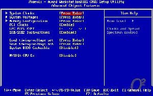
Here is where all the magic happens, the overclocking magic that is. This section is broken up into three nice sections consisting of System Clocks, System Voltages, and Memory Config. This layout is kind of nice and should lead to easy manipulation from within the BIOS because it actually makes sense as to where everything is located.

Beneath the main sections are a few options, three of which deal with saving/loading timings and voltages. The options to save to four different profiles is a welcome sight but it appears to be just the Advanced Chipset Features that get saved and not the entire BIOS like the Genie BIOS of the DFI LanParty series. It would have been nice if the entire BIOS were savable and we could label the profiles but this is a start and a welcome one. I hope more mainboard manufacturers implement features like this in the BIOS, it can come in very handy late at night.
System Clocks

The System Clocks page is very straight forward with no sublevels. Everything on one screen and as you can see, there is only a slight scroll needed to see it all. Everything is labeled in a manner that makes it very simple to know what you are adjusting exactly.
100-500HTT

The HTT actually goes as low as 100 which is a first for me to see but is interesting nonetheless. At the high side we get a lofty 500 to choose from. HTT 400 will likely never see any boards sold to the public but just in case a madman with all kinds of dry ice gets a hold of the C51, it can let you select up to a 500HTT.

The CPU multiplier has been stripped slightly with the removal of 1/2 dividers which caused more memory timing headaches than they were worth, good riddance.
PCIe BUS 100-200MHz

With the advent of some incredible bandwidth munching video cards like the 7900GTX 512 and the newest 7950GX2 from NVIDIA, it is no surprise to see that NVIDIA has jumped on the PCIe BUS overclocking bandwagon. The idea is that when overclocked, these BUSes are actually limiting some video cards so an overclock is required for maximum performance. When you plug in certain video cards in the 590 SLI motherboards, this BUS will automatically overclock, much like the EPP settings on certain memory modules.
SPP<->MCP 200-500

The SPP/MCP link defaults to 200 and when the default multiplier is 5 we get the 1000MHz AMD advertises but again, this HT link can be overclocked as well up to an incredible 500 X 5 = 2500MHz. Of course this likely isn't possible or remotely required but again, the option to go sky high is there. The rest of the options in this section are pretty self explanatory with the option to adjust the multiplier of the individual HT links separately. We look at voltages next.
System Voltages

The list on the left outlines what voltages we have control over and there are many. The CPU and memory voltages are to be expected but we also have full control over the various HT links between the SPP<->MCP as well as the SPP<->CPU. Again, this allows us to tailor the voltage requirements of the various components that we are overclocking in the previous section.
CPU Voltage 0.3750V – 1.8500V

The CPU voltage goes to a CPU cooking 1.8500V and when I took the screenshot I had the voltage already up to 1.67V but I certainly don't think I will be putting 1.85V into any CPUs quite yet. This is one of the single most important factors in overclocking a CPU, the voltage supply and the stability of that voltage.
MEM Voltage 1.800V – 2.500V

Like the CPU voltage, I already have more than the defaults going to the memory and I can already confirm that this board has no issues supplying the full 2.5V to the memory. You will be able to see evidence of that in the overclocking section. A voltmod for more VDIMM will only be required by professionals and OCing freaks like myself alike as 2.5V voids most, if not all, warranties out there on DDR2. That wraps up the voltage sections and we can cruise on to my favorite section, Memory Configuration.
Memory Configuration

Again, a single page for all options except this time we have two submenus to visit as well. Some general timings are out here but the meat and potatoes is inside the
Memory Timings
section so we head there but first, notice the SLI-Ready Memory option that is disabled. This is for letting the system use the EPP profiles on the memory should your memory be EPP compatible. When enabled we get the automatic overclock feature of 0-15% CPU overclock. You can see EPP modules in action in my OCZ 2 x 1GB DDR900 Platinum edition XTC EPP review.
Memory Timings

Like so many sections in this BIOS, a single non-scrollable screen is all that is required for all the options that we are offered. Primary timings at the top and the secondary timings below keep it nice and simple for those that aren't as comfortable in a BIOS as myself. Most users will just be adjusting the primary settings while the advanced settings will only be manually manipulated by the memory geeks in the house such as myself. The options are not as extensive as say a LanParty board from the 939 era but there is plenty here to work with to maximize memory.
Drive Strength

For those that do not know, there is more to memory than just timings and voltages. Drive strengths play a huge role in memory stability and performance, especially when you're tweaking and walking that thin line between BSOD and a successful 32M SuperPi run. Again, the defaults will be fine for most, but certain users will welcome a DS selection option in the BIOS, even if it is somewhat limited in its scope. I can tell you right now, these settings will be adjusted for the memory overclocking section… I just love beating on memory.
That wraps up the OCing section of the BIOS and I have to admit, it is quite a promising selection of options and the layout is on par with the DFI LanParty layouts. Foxconn has done very well thus far and I can hardly wait to get to overclocking this setup.
Integrated Peripherals

This section is nothing more than the place to enable or disable any onboard components including hard drives, FireWire controllers, the floppy disc controller, and the HD Audio.

Power Management Setup

PnP/PCI Configurations

System Monitor

The monitoring page doesn't give us any options such as fan control or shutdown temps or anything of that nature. It simply reports what is going on. I like this approach and welcome a single screen that provides all this information. I think my 0 RPM CPU fan speed gives away the fact that I am water-cooling this setup… perhaps it was the 24C CPU temp which is actually quite accurate according to an AMD64 Die Temp reading program within Windows. Needless to say, we have covered every screen of the BIOS, or at least I hope we have. If not then feel free to fire me an e-mail or ask questions in our forums where I would be happy to supply additional screen shots or information for you.
Page 8 : Overclocking
I am not sure about anyone else here but overclocking is the biggest factor for me with a motherboard. I mean, there are other deal breakers, but if a high-end motherboard can't run 300 HTT then it is considered a failure in overclocking in my opinion. 300HTT X 9 only equals 2.7GHz and a very high percentage of 3000+ AMD64s will approach those speeds with correct cooling and voltage. The Foxconn C51 BIOS offers every option we will need for proper HTT, HT, CPU, and Memory overclocking so there will be no excuses, either the board performs or it won't.

I am using the setup to the right shown in the photo above. A full list of specifications can be found in the Test Setup section but as I go through the results I will identify the CPU, memory, and other bits used. Naturally with any motherboard, the first thing needed to find out is the max HTT so I start there. I won't bore you with the details, just the maximum capabilities of the motherboard and any notes that I deem important along the way.
Max HTT Prime Stable = 369*7

As you can see, the C51 is certainly no slouch. In fact, it is right up there with the heavy hitters when it comes to HTT and the ability to overclock. The only issue in getting this high was the fact that I could only get the C51 to POST around the 290HTT mark. After that and I wouldn't get POST and depending on the CPU multiplier used, I wouldn't get POST as low as 285. Booting at 280HTT and using ClockGen or nTune to raise the HTT after that is the only way to go. Here are the voltages used to reach the lofty stable HTT of 369:

Obviously these are not the default voltages and are actually the max the board will offer for the various chipsets. An HTT of about 270-280 was stable on stock voltage and after that, gradual increases were required to stabilize the overclock. The C51 is off to an incredible start and should not be the limiting factor in CPU or memory overclocking. Speaking of which, next up is some shiny
OCZ DDR900 4-4-3-15
. Let's see if the Foxconn can out-clock my Asus M2N32-SLI Deluxe and get this memory over DDR1100 4-4-3-5…
Max 4-4-3-5 32M Stable = DDR1100 @2.5V

The wall seems to be 1080MHz and anything much higher would result in an instant reboot when priming started or a lock-up if a Super Pi run was made. This got me suspicious and no matter how loose the secondary timings were, the result was identical at DDR1080 or higher, regardless of the multiplier and HTT combination I was using with different memory dividers as well. Needless to say, the max 5-5-5-15 stable frequency is the same as the 4-4-3-5 and it might be a motherboard limitation but I doubt it. It could be an Integrated Memory Controller issue with this particular CPU. Either way, I will update if this wall is removed in the future so be sure to check the Overclockers Online forums for that.
Max HT Prime Stable = 300 X 5 = 1500MHz

1500MHz was the maximum, I simply stopped there because my max HTT will not exceed a HT of 1500 with a multiplier of 4 so I can basically leave the HT multiplier on 4 and forget about it. There is still no evidence that a basic system benefits at all from an increase in HT bus but with newer, larger video cards and the new routing on the nForce 500 chipset, the HT overclock may produce increases in certain cases.
I could go on to overclock the SPP and MCP buses as well but the only point of that would be again for high-end SLI action and I just don't have a set of high-end SLI video cards to see if there is any benefit so I will be leaving the SPP and MCP overclocks for a later time, perhaps when I have a set of video cards that can actually use the increased bandwidth on those buses. The final thing I want to look at is what the CPU can actually provide in the way of CPU voltage, not just what the BIOS allows for a setting, but what the motherboard will actually deliver before a voltage modification is required.
Max CPU Voltage (VCORE) = 1.79V BIOS / nTune

This is the most VCORE that this motherboard will put out as measured by the BIOS. I am still hunting for a point to measure VCORE with the DMM to confirm an accurate measurement but it appears that this Foxconn C51 has no problems sending juice to the CPU. I could have in fact gone higher but 1.79V was more than I was comfortable with going to my CPU under just water. Again, I will update when a voltage measuring point is found to confirm that the CPU is actually receiving this massive amount of voltage. Volt mods won't be necessary for all but the most crazy of overclockers and without sub-zero temperatures, you are crazy to use this much voltage. Next is the memory voltage supply… and the news is good there as well.
Max Memory Voltage (VDIMM) = 2.5V BIOS / nTune / digital multi-meter

Unlike the VCORE reading, a VDIMM measuring point was easily identified on the motherboard and I could confirm that the memory was actually receiving the BIOS or nTune selected voltage, and quite stable voltage at that. The maximum of 2.5V that was selected is bang on according to my digital multimeter. At this point, I am ready to wrap up the overclocking section with the maximum stable CPU and overall overclock that will be used for testing alongside the stock 2GHz results.
Max System/CPU Overclock = 300HTT x 10 = 3GHz CPU / DDR1000 4-4-3-5 2.3V / 5 x 300 = 1500MHz HT

To keep the review moving I will spare the meatloaf and get to dessert. The key to this overclock is the fact that the IHS (Integrated Heat Spreader) was removed and my Asetek WaterChill CPU waterblock was mounted directly on the core, reducing temperatures drastically in this situation and allowing for an extra bump to 3GHz Prime, Super Pi 32M, 3D benchmarking, and game stable. The CPU tops out shortly after that regardless of voltage and other settings so it just seems to be done at 3GHz. This will obviously not be the average overclock for AM2 3200+ processors so I will do the overclocked testing at
2.7GHz / DDR900 4-4-3-5 / HT 1.5GHz
. This overclock is still on the high end but both my 3200+ and 3500+ CPUs will run 2.7GHz on aftermarket air coolers in more than one motherboard so I think many will get these kind of clocks on this fine motherboard.
Page 9 : Test Setup
AMD Athlon64 3200+ (LLBVE 0617XPXW)
Asetek WaterChill
OCZ 2 X 1GB OCZ29002048 (4-4-3-5)
HIS X800GTO IceQ II Turbo 256MB 570MHz core / 600MHz memory – Catalyst 6.1
SilverStone Zeus ST56ZF
36.6GB WD Raptor 10,000RPM
Windows XP Pro SP2 + with all available updates
Components will be spread out across my desk for testing.
Control Socket 939:
AMD Opteron 146 (CAB2E 0546GPAW)
Thermalrite XP-120 heatsink w/Vantec Stealth fan
OCZ 2 X 1GB OCZ5002048EBPE-K (2-3-2-7)
HIS X800GTO IceQ II Turbo 256MB 570MHz core / 600MHz memory – Catalyst 6.1
SilverStone Zeus ST56ZF
36.6GB WD Raptor 10,000RPM
Windows XP Pro SP2 + with all available updates
Components will be spread out across my desk for testing.
Motherboards:
Foxconn C51XEM2AA-8EKRS2H
– nForce 590 SLI chipset / ForceWare 9.35
ECS KA1 MVP Extreme – ATI RD480/SB450 chipset
DFI Infinity NF4 Ultra – NVIDIA nF4 Ultra chipset / ForceWare 6.66
Foxconn NF4SK8AA-8EKRS – NVIDIA nF4 SLI chipset / ForceWare 6.66
Asus A8V-E Deluxe – VIA K8T890/VT8237 chipset
Page 10 : System Benchmarks
My motherboard benchmarking suite includes the usual memory bandwidth and latency testing thanks to Everest Ultimate 06 and SiSoft Sandra Pro SR3. I chose not to switch over to the SiSoft Sandra 2007 as its results differ greatly from the 2006 version and all the 939 motherboards were tested with the 06 version. ScienceMark 2 was also included, as always, and one of my favorite benchmark programs, SuperPi, will be included as well with 1M, 2M, and 32M runs. HD Tach will be used for testing the hard drive performance but the biggest disappointment for me will be the inability to test RAID0, RAID1, and RAID5 numbers due to a lack of hard drives on hand. Look for an update on those numbers down the road when the hard drives become available. TO wind up the system benchmarks, I will run Futuremark's PCMark04 and 05. Let's see how AM2 and the nForce 590 SLI runs up against socket 939.
Everest Ultimate 06 2.50.480

The memory benchmarks are of most interest to me as it will be the first time I get to see the difference between DDR2 and DDR. So far, the latency appears to suffer a slight bit at stock speeds of DDR800 and DDR400. Switching to bandwidth on the read and write appears to be a split decision which is a bit odd to see. At DDR1000 with a higher clock speed, the DDR2 numbers walk away from DDR400 but keep in mind the CPU frequency plays a large role in that.
SiSoft Sandra Pro SR3


The SiSoft Sandra numbers group both of the stock settings very close together with almost identical results but DDR800 appears to have a slight bandwidth lead over DDR400.
ScienceMark 2

The ScienceMark results show a decided advantage to the AM2 platform with DDR800 and looser timings. Even at the same CPU frequency, the DDR2 rockets past the DDR numbers despite looser timings.
Super Pi Mod 1.4

SuperPi isn't exactly a real-world benchmark but it does properly gauge the systems ability to do pure number crunching and there doesn't appear to be any differences between the socket 939 results and the socket AM2 numbers. Even running a 32M digit calculation results in similar times amongst the motherboards.
HD Tach 3.0.1.0

The SATA hard drive numbers are again, very similar to the 939 results which leads me to believe there won't be any significant gains in real-world apps going AM2 vs. 939. I really wish I could have tested the RAID performance but something tells me when I do, we won't see too much difference.
PCMark 04 v1.3.0/05 v1.1.0

After looking at similar numbers throughout testing, I fully expected to see PCMark04 / 05 numbers just as close, and naturally they are. I think it is safe to say there isn't any performance decrease from the switch to DDR2 memory but there sure aren't any significant performance gains at stock speeds either. Keep in mind I am also running a fairly high-end kit of memory and with a generic set of DDR667 or DDR533, you will see even less performance from the socket AM2 lineup. We will now take a look at some gaming performance numbers before wrapping this review up.
Page 11 : Gaming Benchmarks
No motherboard review is complete without some gaming benchmarks. In the synthetic benchmarks above there were no real gains seen so I don't expect miracles with the gaming results either but that extra bit of bandwidth the DDR2 seems to be pushing may help slightly.

Through 3DMark06 down to 03 there isn't much difference between the stock 2.0GHz settings amongst the five motherboards and that is mostly due to the GPU being the major player in determining the score but in 3DMark2001, we see the C51 dip a bit compared to the 939 motherboards. This might indicate some system weakness in the AM2 platform when compared to 939 for gaming. The next chart showing benchmarked results of actual gameplay will hopefully shed some light on this dip in 3DMark2001.

Well, it isn't exactly decisive but it appears that the AM2 board might not be as well a performer compared to 939 at the stock settings with memory at only DDR800 with fairly tight timings of 4-4-3-5 compared to DDR400 2-3-2-7. HL2 is the obvious standout that shows a substantially weaker performance than the other two games. Like I said, this wasn't a comprehensive gaming performance review but it might show that DDR2 still has a bit to go before matching tightly timed DDR performance.
Page 12 : Conclusion
Foxconn was given the task of designing one of the early socket AM2 NVIDIA 590 SLI motherboards and did so well that NVIDIA choose it as the reference design. The layout lacks any faults with all connections to the outside, leaving plenty of space for the memory and CPU socket area for large coolers. The two PCI-E X16 slots are spaced far enough apart to allow for any NVIDIA SLI configuration, which is sometimes an issue on other designs. Overall, the layout is a no-frills approach that gives us, the end-user, plenty of options to suit our needs.
This review was as much about the Foxconn
C51XEM2AA-8EKRS2H
, as it was about the new NVIDIA 590 SLI chipset, and I was a bit disappointed to see very little, if any, advantage of the 590 SLI chipset when compared to the older nForce4. That said, there is very little drawback going to the new 590 chipset as driver availability is there for 32-bit and 64-bit Windows, and the performance did show some signs of optimism. The most impressive results come in the overclocking section, especially with the memory.
The BIOS options are deep enough to allow veteran overclockers the ability to tune the system for large overclocks and the basic user has enough features to allow them an easy and stable overclock as well. The combination of NIVIDA EPP memory and other enhancements to the features offered make the Foxconn "C51" an excellent choice for that jump to socket AM2. I look forward to upgrading the CPU to a dual-core and adding a pair of quality video cards in the near future so look for more work from the
Foxconn C51XEM2AA-8EKRS2H
.
Advantages
Impressive overclocking ability
Driver availability and quality as good as nForce4
Subtle enhancements from nForce4
Solid layout giving room where needed
Disadvantages
Performance over nForce4 is small, if any
High-end DDR2 costs more than high-end DDR right now
I would like to thank Foxconn for providing the sample for review.